Process
From the first feasibility memo to FOTA patches three years after launch — one team, one accountable timeline.
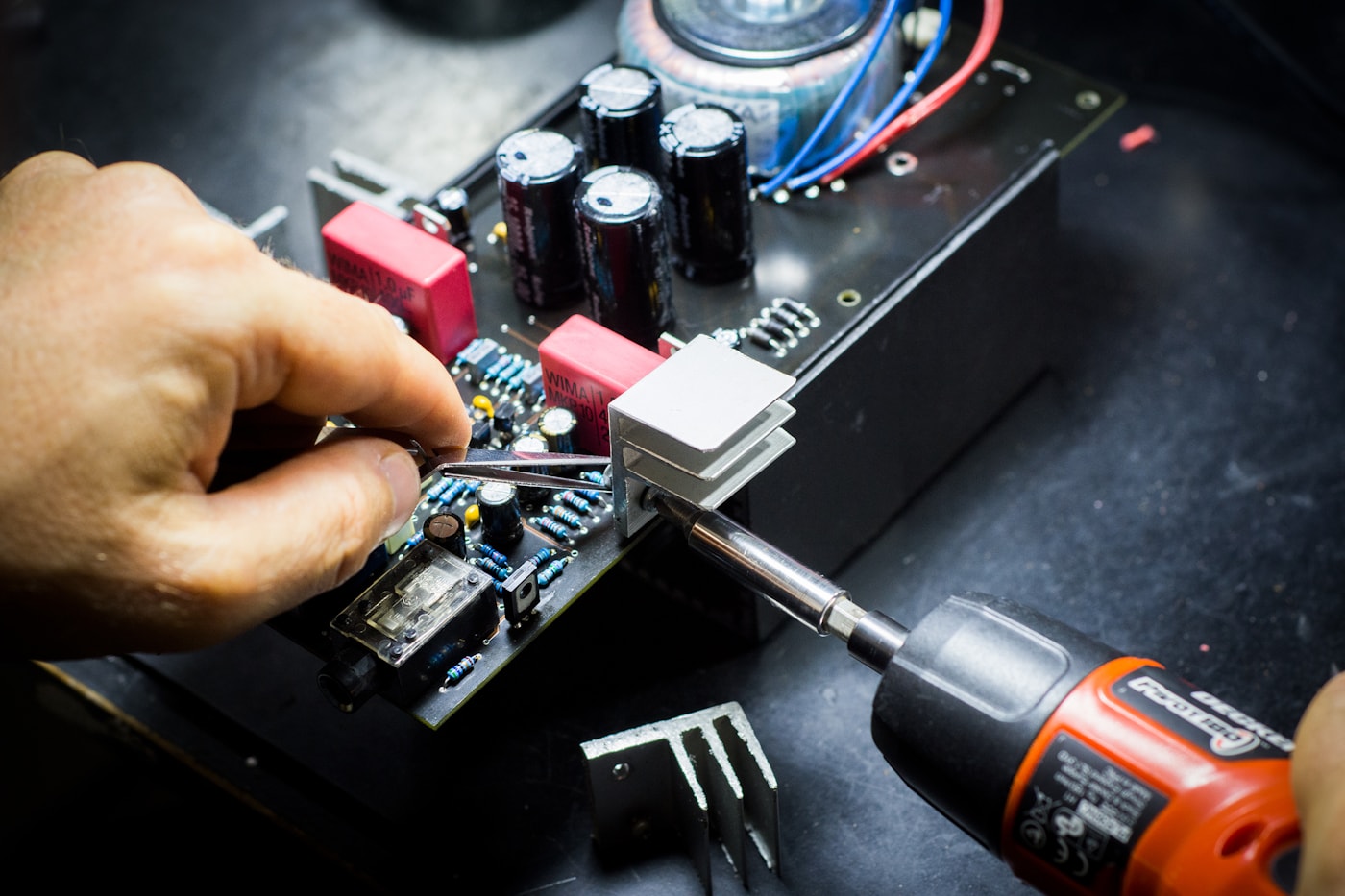
Six steps. One supplier. One accountable team.
From requirements and component selection to prototype validation and production, reduce the back-and-forth between hardware, software, and factory teams. One team works to the same product specification, cost target, and schedule.
- 01
Discovery
Week 1We discuss product requirements and functional specifications, clarify expected sales volume and cost targets, and deliver a feasibility memorandum within the first week.
- 02
Architecture
Week 2–3Block diagram, module selection, MCU & sensor shortlists, antenna and power budgets, mechanical concept. Reviewed against a compliance checklist.
- 03
EVT prototype
Week 4–7First PCBA + tooled enclosure. Firmware up to bring-up. Internal field testing and RF pre-scan in our anechoic chamber.
- 04
DVT & certification
Week 8–12Validate the design against your specification and define testing and certification scope for the target market. Export projects can plan testing against relevant CE, FCC, RED 3.3(d/e/f), ETSI EN 303 645, RoHS, and REACH requirements.
- 05
Mass production
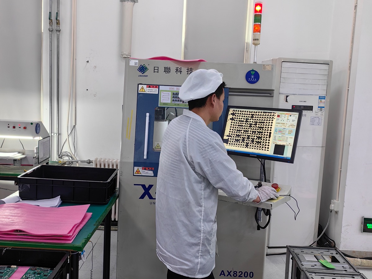
Week 13+PVT, then ramp. SMT, assembly, programming, calibration, packaging in our Shenzhen line. ISO 9001 / 14001 audited.
- 06
Sustaining
OngoingFOTA fleet management, field RMA, BOM watch, EOL tracking, security patches. We stay on the hook for the life of the product.
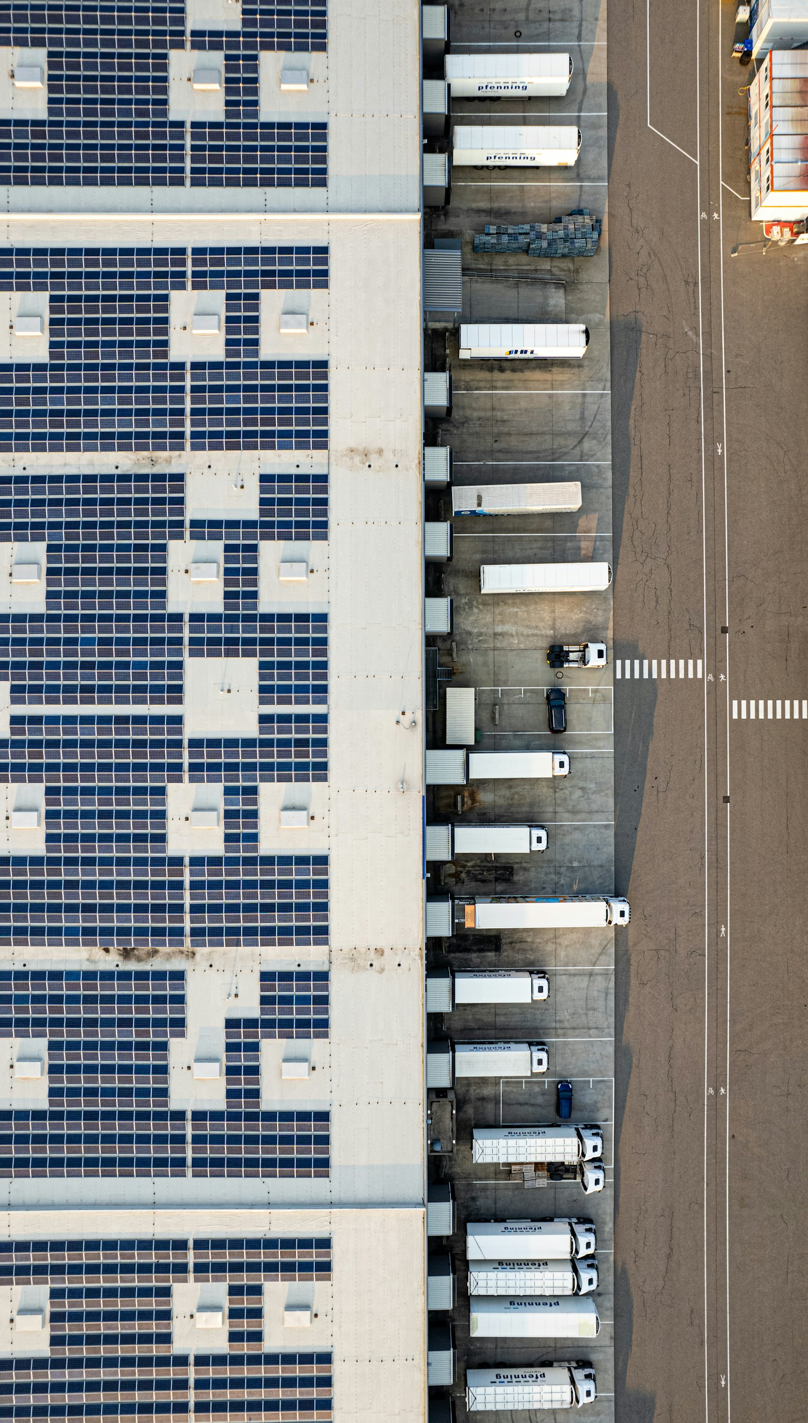
A real factory, not a forwarding address.
Our Shenzhen facility is ISO 9001 / 14001 certified. Two SMT lines, two assembly lines, RF pre-scan chamber, IPX/IK drop testing, climate aging chambers, and a small-batch tooling shop.